
How UK PCB Assembly Is Being Transformed by 5G, EVs and Miniaturisation
The UK electronics manufacturing sector is in the middle of a rapid and far-reaching transformation. As new technologies such as 5G communications, electric vehicles (EVs) and compact, highly integrated devices become mainstream, the expectations placed on printed circuit boards (PCBs) have never been higher. Boards must now cope with faster data rates, higher power densities and more demanding operating environments, often within smaller physical footprints.
For UK-based PCB assemblers and contract manufacturers, this shift presents both pressure and opportunity. On the one hand, customers expect shorter lead times, improved traceability and consistent quality across every batch. On the other, there is a growing appetite for local, technically capable manufacturing partners who can understand complex designs, advise on manufacturability and deliver dependable results across the full product lifecycle.
In this article, we look at three of the strongest forces reshaping PCB assembly in the UK today: the rollout of 5G infrastructure, the growth of the EV and charging ecosystem, and the ongoing drive towards miniaturisation in sectors such as medical, industrial and consumer electronics. Each trend is pushing assembly processes, equipment and engineering practices in new directions.
Whether you are an electronics designer, engineering manager or buyer responsible for sourcing PCB assembly in the UK, understanding how these changes affect manufacturing will help you make better long-term decisions about suppliers, technologies and production strategies.
Many of the most important developments are happening not just at design level, but on the production floor. Modern surface mount technology (SMT) lines are moving towards finer pitches, smaller passive components and more demanding thermal profiles. At the same time, quality expectations and regulatory requirements remain high, especially in sectors such as automotive, medical and defence.

5G Technology and High-Frequency PCB Requirements
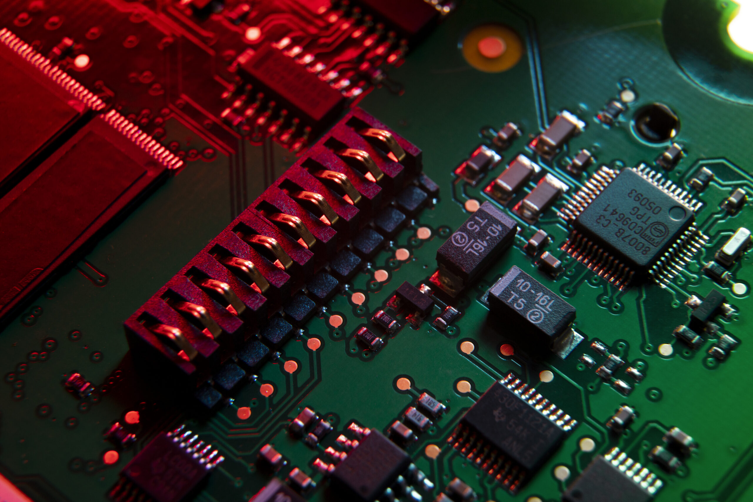
The arrival of 5G has dramatically increased the technical demands placed on PCB assemblies. Operating at far higher frequencies than 4G, 5G systems require carefully controlled PCB stack-ups, low-loss substrates and extremely consistent manufacturing. Signal integrity is crucial. Even small variations in trace width, dielectric thickness or solder mask can impact performance at multi-gigahertz frequencies.
To support this, many UK manufacturers are working more regularly with advanced laminate materials that have tighter dielectric tolerances and more stable performance over temperature. These materials behave differently from traditional FR-4 during soldering and reflow, so process windows must be adjusted and controlled carefully. Thermal profiles, preheat stages and cooling gradients all need to be calibrated to prevent warping, delamination or joint issues.
Component density is also rising. RF front-ends, filters, matching networks and antenna arrays are now packed into tightly constrained spaces. This demands very accurate SMT placement and consistent solder paste application. Stencil design, aperture reduction and paste type selection all play a part in ensuring that fine-pitch components and tiny passives reflow correctly, with no bridging, opens or unintended voids.
Inspection has become more important than ever. Automated optical inspection (AOI) systems are now expected to detect very small errors in solder joint geometry, component skew and polarity. For hidden joints, such as those used under BGA and LGA packages, X-ray inspection and controlled rework processes play a crucial role. When a board is destined for telecoms infrastructure or critical networking equipment, there is little room for intermittent faults or latent defects.
Ultimately, 5G is nudging UK PCB assembly into a more precise, more tightly controlled era. Manufacturers able to invest in both equipment and people will be best placed to support the wave of 5G-enabled products entering the market.
Electric Vehicles and High-Reliability PCB Construction
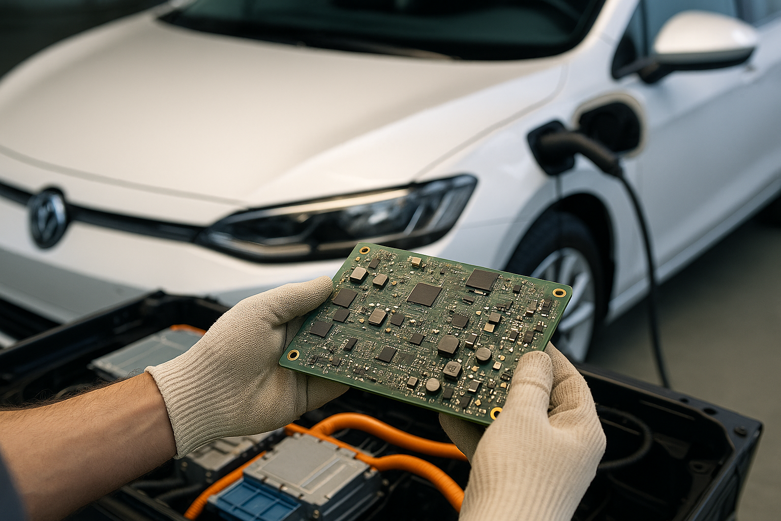
The growth of electric vehicles is another major driver of change within UK PCB assembly. EV systems depend on a wide variety of electronic control units, from battery management systems (BMS) and inverters to onboard chargers, thermal control modules and infotainment units. Many of these assemblies must operate reliably under conditions that would quickly expose weaknesses in design or manufacturing.
Automotive-grade electronics must routinely withstand vibration, shock, wide temperature swings and exposure to moisture or contaminants. As a result, PCBs used in EV applications often feature heavier copper weights, reinforced substrates, additional mechanical support and carefully chosen conformal coatings. Solder joints must be strong enough to handle thermal expansion and contraction over many years of service.
From an assembly standpoint, this means that both SMT and through-hole processes must be tightly controlled. Large connectors, high-current terminals and power components frequently rely on through-hole soldering to provide mechanical security. Surface-mounted power ICs and gate drivers require precise thermal management and clear solder fillets to guarantee performance.
Reliability expectations are extremely high in this sector. Failures in EV battery control, power distribution or safety-related electronics can have serious consequences. This makes inspection and test processes essential. In-circuit test (ICT), functional testing, burn-in and environmental stress screening are often used in combination to validate assemblies before they are integrated into vehicles.
For UK manufacturers, the growth of the EV industry is a significant opportunity. Those who can demonstrate robust quality management, strong process control and the ability to work closely with automotive engineering teams will be in a strong position to support both vehicle manufacturers and tier suppliers.
Miniaturisation and High-Density PCB Assembly
Alongside 5G and EVs, there is a continued push towards smaller and lighter electronic products. From wearable medical sensors and handheld diagnostic equipment to industrial IoT nodes and compact control modules, many applications demand PCB assemblies with very high component density.
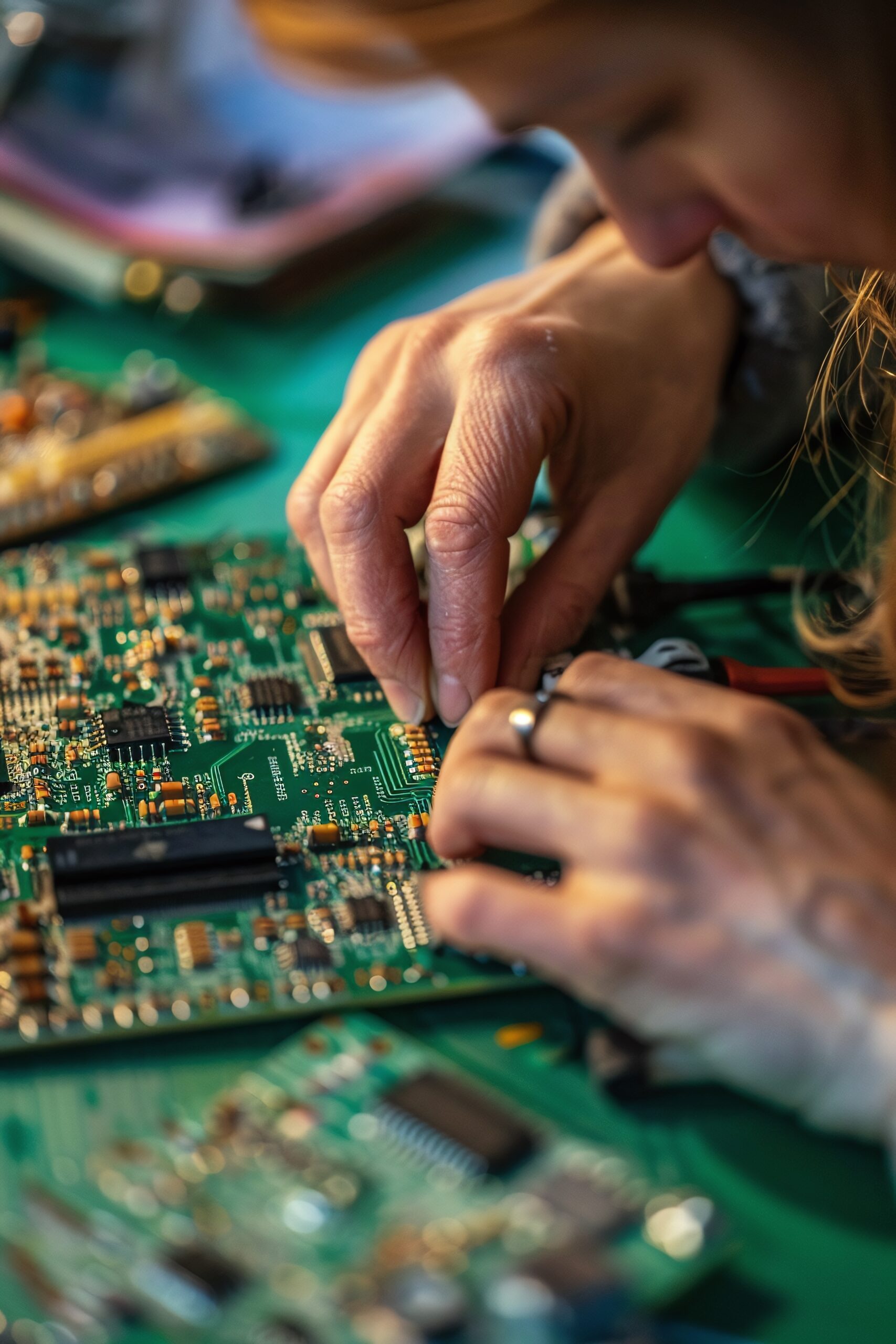
This has led to the widespread use of tiny passive components such as 0402, 0201 and even 01005 packages. Handling these parts reliably requires modern SMT pick-and-place machines with excellent repeatability and well-controlled solder paste processes. Stencil design, paste type, reflow profile and PCB finish all need to work together to ensure that miniature components wet correctly and remain in position.
Miniaturisation also increases the reliance on multi-layer boards and advanced via structures such as microvias and via-in-pad technology. These features allow designers to route complex circuits within a small footprint, but they also demand high-quality fabrication and careful assembly to avoid issues such as voiding, trapped flux and thermal stress.
Inspection also becomes more demanding as parts get smaller. Solder joints may be tiny, and defects are often difficult to see without proper magnification and automated inspection. AOI systems must be programmed carefully to distinguish between genuine defects and acceptable variations. In high-reliability environments, additional manual inspection under microscopes is often used to validate the most critical parts of an assembly.
For UK manufacturers, miniaturisation is both a technical challenge and an opportunity to demonstrate capability. A facility that can handle fine-pitch, high-density assembly with confidence immediately stands out to designers developing next-generation products.
What This Means for UK OEMs, Designers and Buyers
For UK-based original equipment manufacturers (OEMs), design houses and engineering teams, these trends highlight the importance of choosing the right PCB assembly partner. It is no longer enough to look only at unit cost or headline lead time. Capability, process maturity and communication are just as important.
A good manufacturing partner should be able to:
- Handle fine-pitch SMT and high-density layouts with confidence.
- Advise on materials and stack-ups for high-frequency or high-power applications.
- Offer flexible support for prototypes, small batches and production builds.
- Provide robust inspection and test processes, including functional testing where required.
- Work collaboratively when issues arise, rather than simply building to file and moving on.
Because 5G, EV and miniaturised products often operate in safety-critical or harsh environments, the cost of field failures or product recalls can be extremely high. Partnering with a UK manufacturer who understands these risks and has built processes around mitigating them can significantly reduce long-term project risk.